GigaBaudics
FEATURES
- 0 to 5 Gb/s operation
- 5, 10 or 20 ps step size
- 10 bit delay range
- 85 ps rise/fall times
- Less than 10 ps jitter, <5 ps typical
- Adjustable input threshold range
- Differential ECL outputs
- High-speed remote programming
PRODUCT DESCRIPTION ... SPECIFICATIONS ... PROGRAMMING ... CIRCUIT DIAGRAM ... POWER REQUIREMENTS ... PRICING AND AVAILABILITY ... HOME PAGE
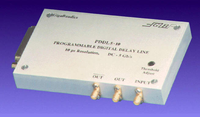
The PDDL5 is a precision time delay generator for digital signals. Delays are controlled precisely in 5, 10 or 20 ps increments from 0 to 5115, 10,230 or 20,460 ps range respectively. Data rates up to 5 gigabits per second are supported for very high-speed applications. Delays can be programmed via a TTL bus.
In GaAs and ECL IC and system testing, the most critical problems involve precisely shifting the relative timing of two or more high-speed signals. The relative timing of two signals may need to be varied in order to determine or to satisfy the critical timing parameters of some high-performance ECL and GaAs systems. High accuracy and high data rates make the PDDL5 well suited to meet the test requirements in bench-top or high-speed ATE systems. A low hysteresis strategy, that reduces variation in threshold crossing as a function of duty cycle or run length, provides a high degree of accuracy at all data rates and delays. DC coupling is used to provide accurate timing control for systems with varying duty cycle such as NRZ and burst data applications. Fast 85 ps rise/fall times and low noise transitions enhance its accuracy. The PDDL5 has differential ECL outputs, which may be used, independently, as single-ended outputs.
Unlike delay generators that employ ramping techniques or multistage active devices for delay generation, the PDDL5 uses the delays produced by using passive GaAs switches to select a binary tree combination of fixed length transmission lines. As a result the PDDL5 has an extended range and can go beyond delays that are less than 1 period in length. Also, passive switches have the advantage of not causing added hysteresis unlike delay lines that use active devices for line switching. Hysteresis is further reduced by compensation techniques. As a result, the delayed signal exhibits very low jitter. The PDDL5 is much more reliable, has faster state changes, higher range and is much less expensive than mechanical delay lines.
High-speed, TTL compatible advanced CMOS latches and control logic has been used for applications requiring very rapid delay-state changes. This allows delay-state changes in less than 30 ns (with a 20 ns propagation delay), that is, programming speeds in exceeding 30 MHz are supported.
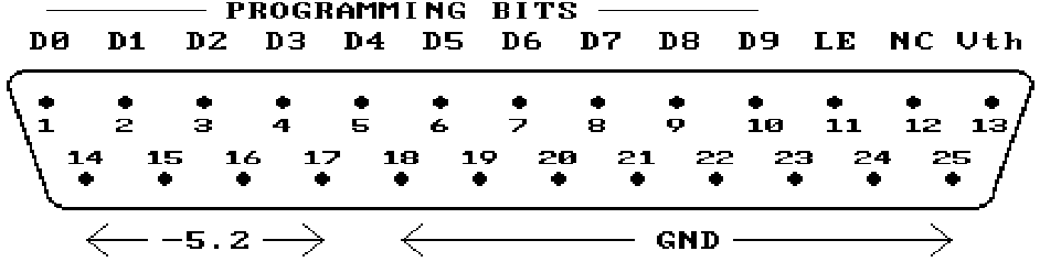
The delay state has a 10 bit programming range. Each of the 10 programming bits (D0-D9) corresponds to a binary weighted delay giving a total of 210 = 1024 possible delay combinations and delay range of 1024 times the step size of either 5, 10 or 20 ps. To program, bring latch line "LE" high, apply the desired delay code to bit 1 through 10, then bring LE low to latch the data. If latching is not desired simply keep the latch line high and the device state will follow the applied data
PIN CONNECTIONS
|
Pin diagram for 25 Pin, male, D-Sub Connector |
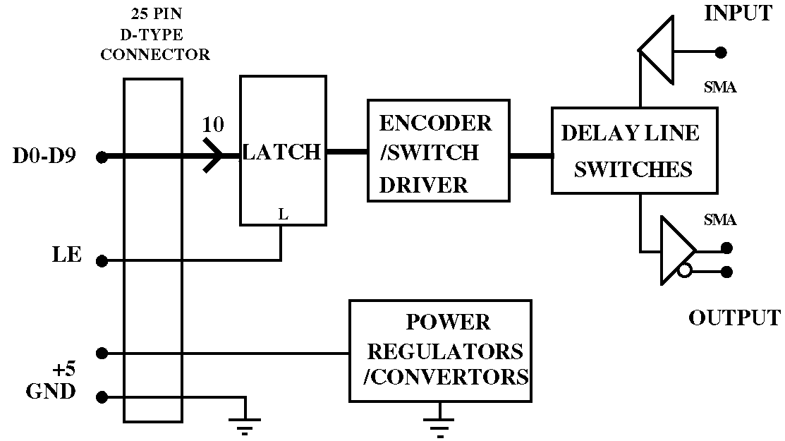
The input and the differential outputs are ECL compatible and connected by SMA jacks. The input is internally terminated to Vtt=-2.0 with a 50 ohm shunt resister. The output voltage swing is 0.8V with Vol=-1.7 and Voh=-0.9. The output is capable of sourcing current only. For proper operation, outputs require a 50 ohm termination to -2.0V. The threshold adjuster may be used to vary the input threshold by +/- 0.4V. This enables fine-tuning of the signal duty-cycle.
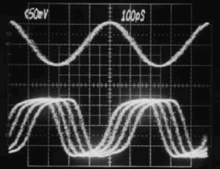
Input (top) and 4Gb/s output (bottom) with 40ps steps.
The PDDL5 is powered by a single -5.2 +/-0.05V supply. Internal supply voltages are regulated to reduce the required number of external supplies and to reduce the level of supply noise appearing on signal path. This improves threshold variation with changes in supply voltages effectively reducing supply noise to the signal. Power is provided either via a standard banana jack or by the D-type connector. Pins 14 through 17 are -5.2V and pins 18 through 21 are GND. Caution should be taken to control the power supply voltage drop if a ribbon cable is used by minimizing the cable length and by using heavy gauge wire. Total power dissipation is typically 0.7 watts. Power dissipation can increase up to 2 watts for rapid programming rates. It is recommended that 1.0 amp. external current limiting be provided since this device has limited over-voltage and reverse voltage protection. For typical applications no thermal management is required. In many cases GigaBaudics can modify the input specifications, the output drive characteristics or the delay step size to help meet the special requirements of the customer, often at no additional cost. Please contact GigaBaudics if there are questions and we will be happy to provide you with further information or clarification.
Price: PDDL5-5; $3240, PDDL5-10; $3780 _____Price subject to change without notice.
Please use e-mail for any correspondences, either technical or administrative, at address postman@gigabaudics.com
![]() GigaBaudics
5266 Hollister Ave. Ste 221 ●
Goleta, CA 93111 ● (805) 687-5934
GigaBaudics
5266 Hollister Ave. Ste 221 ●
Goleta, CA 93111 ● (805) 687-5934