GigaBaudics
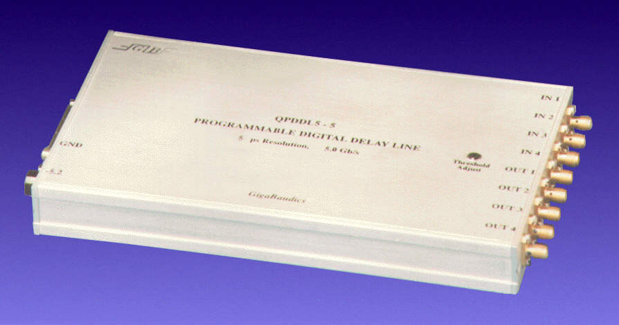
5 Gb/s PROGRAMMABLE DIGITAL DELAY LINE - MODEL SERIES QPDDL5
Features
- 0 to 5 Gb/s (2.5 GHz) operation
- Four independent channels
- 10 bit programmable
- 5 or 10 ps step size
- 85 ps rise/fall times
- Less than 10 ps jitter, 5 ps typical
- Low hysteresis
- High accuracy
PRODUCT DESCRIPTION .... SPECIFICATIONS .... PROGRAMMING .... CIRCUIT DIAGRAM .... POWER REQUIREMENTS .... PRICING AND AVAILABILITY .... HOME PAGE
The QPDDL5 series delay lines are four channel precision time delay generators for digital signals. Delays are controlled precisely in 5 or 10 ps increments at data rates up to 5 billion bits per second or clock rates exceeding 2.5 GHz. Each of the four channels is independently programmable.
In GaAs and ECL IC and high-speed systems testing, the most critical problems involve precisely shifting the relative timing of two or more high-speed signals. The high accuracy and high data rates of the QPDDL5 series make it well suited to meet these requirements in bench-top or high-speed ATE systems. Fast, 85 ps rise/fall times and low noise transitions and a well matched 50 ohm input termination enhance its usefulness in precise timing control. Applications include high-speed pulse-width modulation, timing measurements, error-rate test systems, pulsed-laser timing, RF phase modulation, data/clock synchronization, signal de-skewing and other applications involving precise signal time-alignment. The QPDDL5 models are capable of very rapid delay-state changes (exceeding 30 MHz) for "zero-wait" operation in high-speed automated test environments.
The QPDDL5 series employs GaAs passive microwave switched-line techniques where delay segments are combined from a binary tree. A low hysteresis strategy provides a high degree of accuracy at all data rates and delays by minimizing data-dependent delays. DC-coupling in a wide-bandwidth 50 ohm environment provides the user with accurate timing control for systems with varying duty cycle such as NRZ and burst-data applications. Unlike delay generators which use ramping techniques for delay generation the QPDDL5 has very low jitter (<5 ps) and is not limited to delays that are less than one period in length. The delay range for the QPDDL5 -5 and-10 is 5115 and 10230 ps respectively.
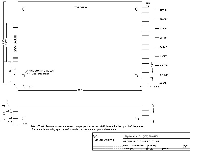
SMA jacks are used for the delay line inputs and outputs. The TTL control inputs include 4 address, 10 programming, device enable, and write enable lines. These are accessed through a 25 contact "D" type connector plug. The QPDDL5 is powered by a single -5.2V supply accessed either by the D-type connector or by the power feed-through jacks.
GigaBaudics also provides the similar QPADL3 series DC to 3.0 GHz programmable delay lines for analog signals.
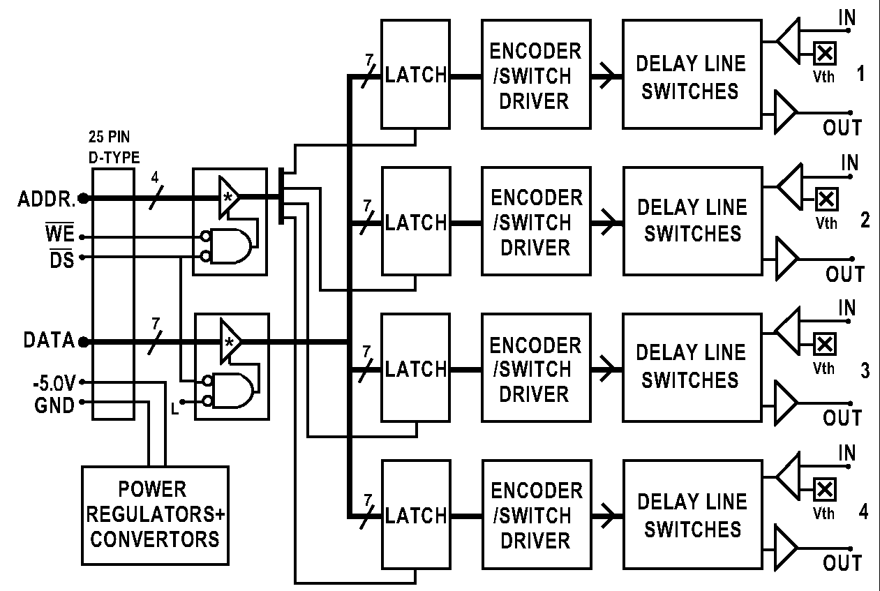
The programmable delay blocks consist of passive microwave line switches in a binary weighted series switched-line configuration. Input and output drivers are specially designed to exhibit low hysteresis. The control logic consists of fast ACT CMOS
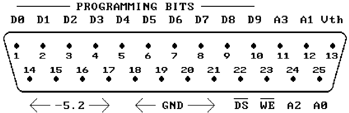
The 10 programming bits are binary weighted delay giving a total of 210 = 1024 delay steps with either 5 or 10 ps step sizes. Each channel is addressed (selected) by a separate address line. This allows any combination of channels to be programmed simultaneously. The WE (write enable) line is activated (low) while the data is valid. The DS (device select), active low, line is a useful for selecting a particular unit when more than one delay-line units are used in conjunction. Data and address lines should be held valid for at least 4 ns and should remain valid 3ns after WE goes high. The control word need not be latched if the user wishes to operate latches transparently. Simply keep the address line high, DS and WE low and the device state will follow the applied data.
Fast, advanced high-speed CMOS control logic is used in this instrument for applications requiring rapid delay-state changes. For particularly high-speed programming applications, option "T" can be used to provide 110 ohm terminations into the TTL input threshold voltage for the control signal lines. This minimizes control signal reflections. For applications requiring delay-state programming rates in excess of 30 MHz, contact the manufacture.
|
PIN DIAGRAM
25 pin, male, D-type subminiature connector |
Inputs are ECL compatible with threshold at -1.3 V. They are connected by SMA and 50 ohm terminated to -2.0 V. Inputs should be driven by at least 0.4 Vpp and have a slew rate >2.0 V/ns for proper operation. A single input threshold adjuster is provided to vary the input threshold -1.3+0.4 V. on all channels. Option V provides individual input threshold adjusters which may be used to vary the input threshold of each channel independently . These threshold adjusters enable fine tuning of the signal duty-cycle.
Outputs are ECL compatible with Voh=-0.85 and Vol=-1.75 and output rise/fall times (20 to 80%) of less than 85 ps. The insertion delay is about 2.2 ns. The insertion delay of each channel is matched so that signal skewing between channels is < 15 ps. This often simplifies installation by eliminating the need for special length interconnect cables. Unused outputs should be 50 ohm terminated to ground.
Option "D" provides differential output drivers so that both the true and the inverted data signals are available. This can be a very useful feature if the output is used to drive, differentially, long or otherwise lossy transmission line.
The QPDDL5 is powered by a single -5.2 V supply making it very easy to use. A well regulated (<50 mV ripple) supply is recommended to reduce signal noise even though Vee-to-signal noise coupling is inherently quite weak. All internal supply voltages (except Vee=-5.2) are regulated to reduce the required number of external supplies and to reduce the level of supply noise appearing on signal path. This effectively negates variation of input threshold with changes in supply voltage thereby minimizing supply noise associated jitter. DC-DC converters are used to generate internal voltages.
Power is provided to either a 25 pin D-type plug or the banana jack. Pins 14, 15, 16 and 17 are -5.2 V and pin 18 through 21 are GND. If a ribbon cable is used, caution should be taken to account for supply voltage drop. Minimize the cable length, use all 4 power pins and use a heavy gauge wire. The QPDDL5 is reverse-voltage protected to 2.5 A. therefore the supply should be current limited to 2.0 A. Total power dissipation is typically 3.5 watts but may increase by as much as 2 watts with rapid programming rates.
 |
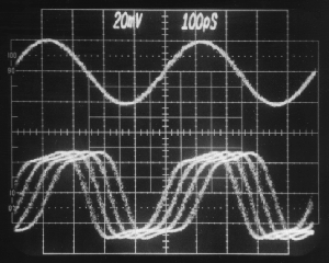 |
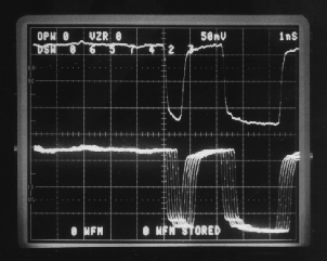
| Photo #1 shows a 1.5 Gb/s input signal (top) and the the delay-line output (bottom) with 100 ps delay increments. Vertical scale is about -15 dB. | Photo #2 shows a 2 GHz input sine wave (top) and the 4 Gb/s delay-line output (bottom) with 40 ps delay increments. Vertical scale is -about 21 dB. |
 |
 |
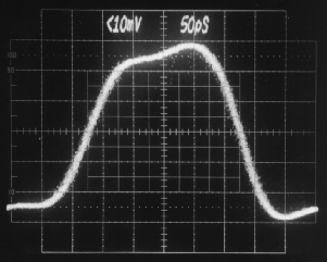
| Photo #3 shows a 4 Gb/s output signal with 20 to 80% rise/fall times of about 70 and 60 ps . |
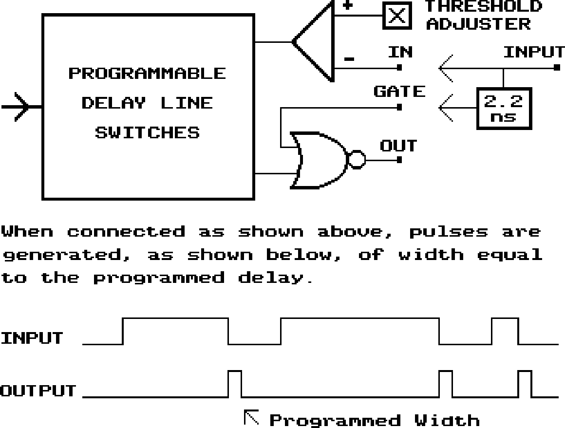
OPTION G |
Option G provides an output driver gate port which can be used to generate pulses of precise widths. If the gate is driven with the "input" signal delayed by about 2.2 ns then pulses (as narrow as 200 ps) are generated of width equal to the programmed delay. If the gates are not connected then the internal input terminations will pull the NOR input low so that the QPDDL5 will operate equally well as a programmable delay or a pulse width modulator.
All TTL and ECL inputs and outputs are static sensitive and caution should be exercised when handling and connecting. No warranty will be extended to damaged inputs or output drivers.
OPTIONS
Option A: Single input driving all 4 channels ($0)
Option D: Differential outputs ($500)
Option I: Inverted data and address control logic ($0)
Option V: 4 Individual input threshold adjusters ($200)
Option G: Output driver gating ports ($500)
In many cases GigaBaudics can modify this product to help meet the customers special requirements. A significant degree of flexibility exists for modifying the input characteristics, output characteristics and the delay step size, often at little or no additional cost. Please contact GigaBaudics for additional information.
If an AC coupled signal generator is used to drive this instrument, keep in mind that the inputs are 50 ohm terminated to -2.0 V. It will be necessary to bias the input voltage such that the signal transitions are centered at the input threshold voltage. This can be accomplished by using a "bias T". A "bias T" has the disadvantage of causing duty-cycle dependent biasing producing data-dependent delays that may appear as jitter. A better approach is to use a 3 or 4 dB pad on the input to offset the input voltage to near threshold. The pad shifts the voltage with its internal shunt resistance to ground. This approach is duty-cycle independent. NRZ or long run-length data sources should be DC coupled to prevent data dependant delays arising from DC voltage drift at the input.
Both the signal source and the output termination should be well matched to 50 ohms over a wide (5 GHz) bandwidth to ensure high delay accuracy. Poorly matched inputs and outputs will generate reflections. Reflections may result in delay-shift aberrations when the signal transitions and reflections are coincident at the point of detection. This often results in what appears to be jitter.
In order for outputs to meet the full specifications outputs should be 50 ohm terminated to -2.0 V. Unused outputs should be 50 ohm terminated to GND.
Delays should be referenced to the input. If delays are referenced to other channel outputs or to the output at 0 ps delay, the two delay errors will add. The "0" ps delay is "just another delay" and has its own error associated with it. This error at 0 ps delay is typically about 3 ps depending upon channel-channel effects. The error of any particular delay can be determined by curve fitting the programmed delay .vs. actual delay and measuring the deviation from the best-fit line.
Should there be any questions or need for clarification please contact GigaBaudics.
Price $ 8640._____ Price and specifications subject to change without notice.
Please use e-mail for any correspondences, either technical or administrative, at address postman@gigabaudics.com
![]() GigaBaudics
5266 Hollister Ave. Ste 221 ●
Goleta, CA 93111 ● (805) 687-5934
GigaBaudics
5266 Hollister Ave. Ste 221 ●
Goleta, CA 93111 ● (805) 687-5934